Function Generator
This device was created for my practical circuit design class at Case Western. Special acknowledgement to my lab partner JC for helping with all these designs.
Specifications
- General Specs
- +/- 15V power rails
- Two frequency ranges: 10-100 Hz and 0.1-1 kHz
- Frequency sweep functionality (10Hz)
- Gate input: generator outputs 0V with a logic low input
- No MOSFETs allowed
- Wave Generation
- Sine, square, and triangle waveforms
- Continuously variable offset: +/- 10 V
- Continuously variable amplitude: 0 to +/- 10 Vpp
- Amplitude adjustment must not affect offset
- Square wave rise/fall time < 100 μs with 10 nF load capacitance
- Sine wave THD < 2%
- Capable of sourcing and sinking 50 mA
- Pulse Generation
- 0 to 12V peak fixed amplitude
- Capable of sourcing and sinking 200 mA
- Rise and fall time < 100 ns
- Duty cycle adjustment ~0 to 100%
Block Diagram
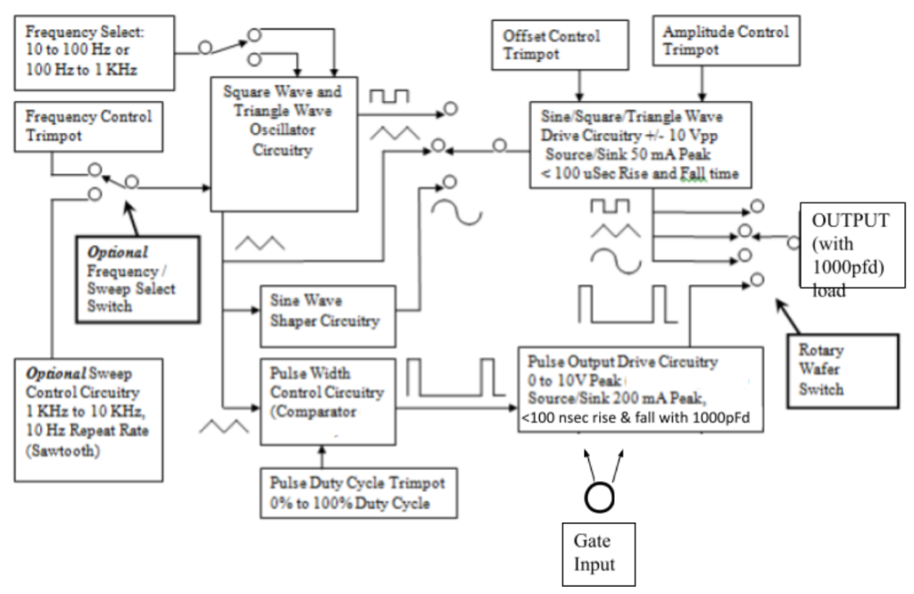
The Design
Oscillator Core
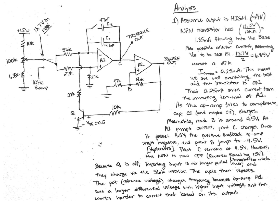
The frequency sweep and no MOSFET requirements limited our selection for oscillators, as we could not adjust the time constant of an RC oscillator with an external signal. This meant we had to use some type of voltage controlled oscillator. Many implementations online utilize a MOSFET for Q1. Given the limitation imposed by the assignment, we decided to give it our best shot with a BJT and it worked out.
The different frequency ranges were accomplished with the use of a latching switch to increase the 4.7 nF feedback capacitance to 51.7 nF. Navigation within these frequency ranges is handled by an external voltage. In the “manual” mode we used a normal potentiometer which was bounded by two resistors to prevent the user from moving outside of the defined frequency ranges as that would cause distortion on the sine wave output. We used another latching switch to select between the manual frequency adjustment and the 10 Hz frequency sweep signal, which was generated with the same oscillator on another part of the board.
An analysis of the oscillator’s function is written below.
Wave Generation
The complete schematic of the oscillator and wave generation stages
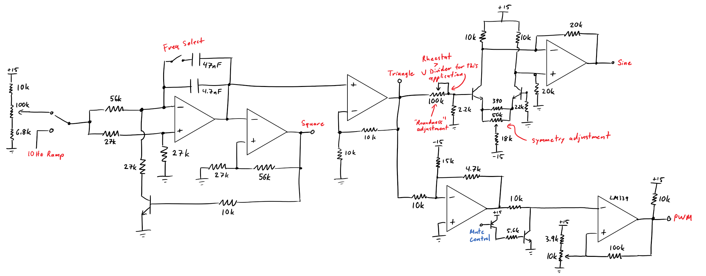
Since our core oscillator generated both a triangle and square wave, the only two shapes we needed to generate were a sine wave and variable width PWM. We found that the slew rate of our operation amplifiers was plenty to satisfy the 100 us rise time limit imposed on the square wave output. In order to avoid potential frequency instability from loading, we buffered the triangle wave and amplified it by a factor of two, bringing its total swing from 10 Vpp to 20 Vpp, giving us head room to reach the 15 Vpp output specification without having to amplify later in the device and potentially introducing additional noise.
Creation of the PWM used to drive the pulse output was rather simple. By offsetting and amplifying the triangle wave such that it is unipolar and lies between 0 and 15 V at all times, we were able to use a basic open collector comparator with an adjustable trigger point to create a square wave with an adjustable duty cycle. This section of the schematic features the “mute control” which we used to accomplish the “gate” functionality of the device, but this aspect will be explained in depth later on. The 100k positive feedback resistor provides enough hysteresis to prevent random switching due to noise on the power line or incoming signal.
The sine wave shaper used here is a bit more rigorous than it had to be. I discovered this implementation several years ago while researching wave shaping for musical synthesizers and decided that I wanted to give it a try in the lab. Details on its operation can be found in this paper by open music labs. In essence the emitter degeneration sine wave shaper uses the turn on characteristics of the BJTs themselves to round off the tops of the incoming triangle wave. Although more professional and thought out implementations of this design have reached well below 1% THD, the closest we were able to get was around 2.3%. This may have been improved with better component selections and replacing the biasing network with a constant current source instead of resistive elements.
Wave Selection & Output Stage
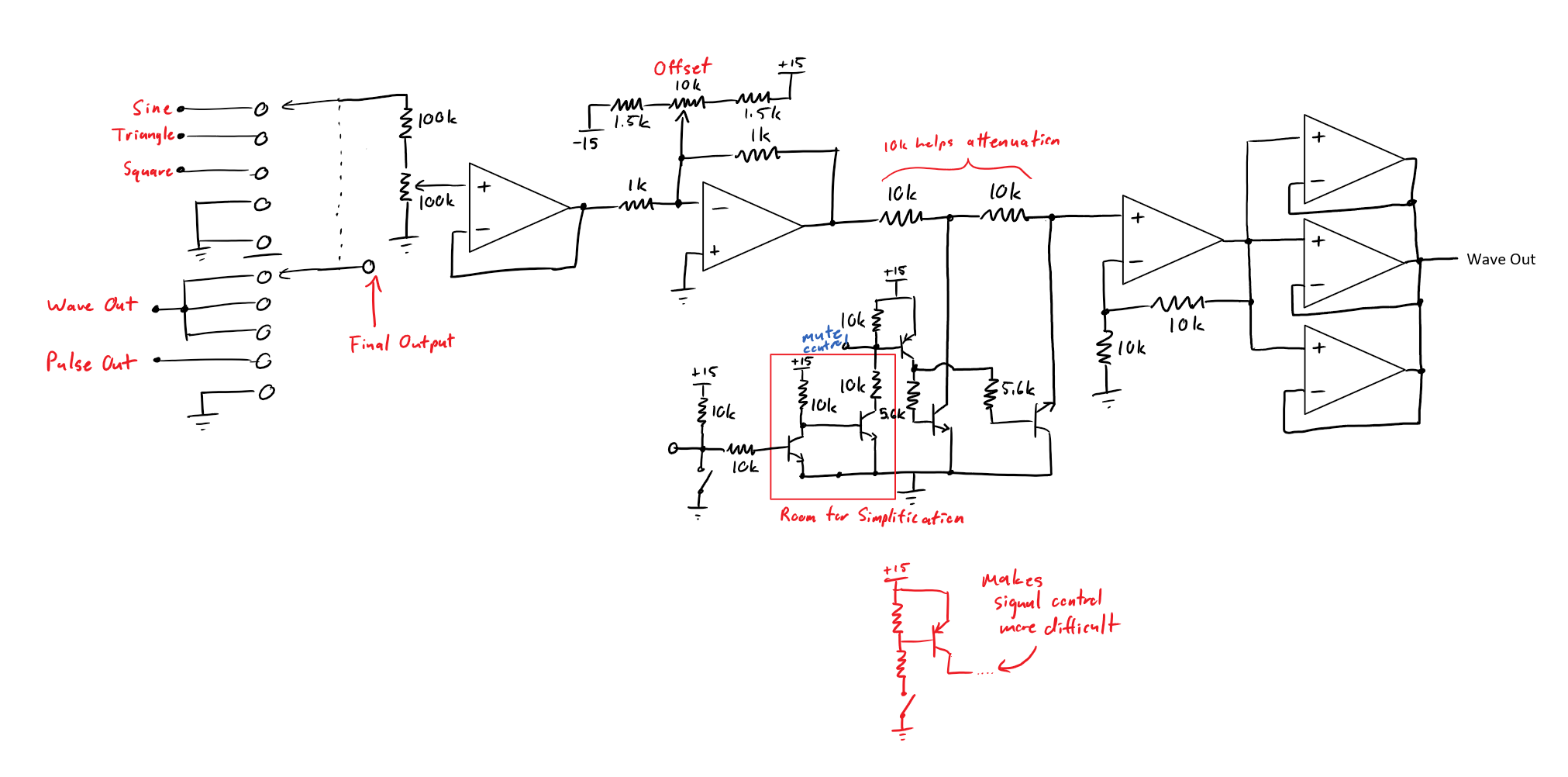
The breadboards used in the lab had a 2P5T rotary switch attached that we were instructed to use for selecting the wave being output. The switch itself was pretty robust so we did not have any issues with passing a few hundred milliamps through the contacts. To accomplish the correct sequence of waves, we had one pole of the switch pass the three basic wave forms through an output stage, and then tie the output stage to ground when the pulse generator was being used so that “Wave Out” node was not left to float around. The second pole on the switch was used as the very last barrier before the output to determine if the wave generator or pulse generator was present on the output of the device.
The output stage for the wave generator is relatively simple. To prevent the amplitude control from affecting the signal offset, we first passed the signal through a resistive divider, then followed it up with an inverting summing amplifier which would add the desired offset to the signal. After the amplitude and offset were determined, we passed the signal through our “mute” circuitry, after which we had to amplify it again (unfortunately). In order to satisfy the output current specification, we used three buffers in parallel. While I wouldn’t call this solution elegant, it saved a lot of brain power in figuring out a proper output stage that wouldn’t introduce and undesired effects such as zero crossing distortion or non-linearity. I believe each amplifier was capable of around 20mA peak output current, bringing our maximum output to around 60 mA.
The muting circuitry here was lifted from some reading on home audio receivers. The “no MOSFET” restriction is a big reason why we went for this relatively odd approach. The idea behind this scheme is that the input bias of the non-inverting amplifier is largely negligible, so we can place a high value resistor in line with the signal without affecting normal operation. When we want to turn off the signal, all we need to do is put a large load after the series resistance to effectively destroy the wave down to a few millivolts at best. This load is applied by the pair of transistors seen below the 10k resistors.
You’ll notice that one of the two NPN transistors appears to be hooked up backwards (HINT: it is). It turns out that BJTs are capable of operating in both directions under the right conditions. Although they are optimized for maximum gain for passing current from collector to emitter, given enough base current they are capable of conducting in the reverse direction as well. Additionally, since we are operating with a relatively low-power system, the BJTs themselves are not at much risk for being damaged.
If you were to only use one BJT, you would get highly asymmetrical attenuation as the positive half of the wave would be destroyed by resistive losses due to the amount of current passing through the BJT (and therefore the 10k resistor) but would be largely intact on the negative swing due to the much smaller gain of the BJT in the reverse direction. This issue is solved with the reversed transistor, however it comes with a rather important caveat. The base of both BJTs must be an open circuit when the mute circuitry is not in use. We accomplished this with a level shifter for the incoming control signal which would activate both BJTs when a logic low input is present on the input, and leave the base of both BJTs floating when not in use since the PNP transistor would allow effectively no current to pass in either direction.
You’ll notice in an earlier figure, we copied this same structure to control the PWM signal. Since this was controlling a completely different node of the circuit, we had to use another PNP level shifter section to keep it isolated from the normal wave gen output stage. With this implementation we found that the output signals were all but annihilated when the mute control was active. Our oscilloscope showed no sign of the signal, even on the lowest available scale.
Pulse Generator Output Stage
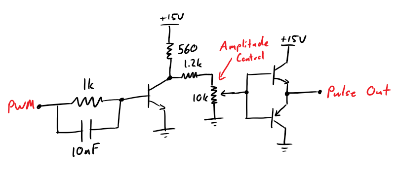
The primary constraints for the pulse generator were a maximum output current of 200 mA and a much faster rise time of 100 ns or less. To accomplish these goals, we could no longer rely on op amps, or even the comparators available to us in the lab. Since we didn’t have to worry about distortion in a digital function such as this, basic transistor configurations can be used. The first stage acts as a sort of buffer, giving us the ability to add an amplitude control and providing an ideal spot to add a “speed up capacitor”. The role of this capacitor is to provide a low impedance path to the base of the transistor right at the rising edge of the incoming PWM signal. This benefits us by turning the first BJT on very quickly, before the PWM signal has completed its own rise time.
After speeding up the incoming edges, we were able to provide 200mA of sourcing and sinking capability with the totem pole configuration on the output, which is reminiscent of many CMOS logic architectures, except flipped. If the incoming signal is high, the NPN transistor on top will be active while the PNP on the bottom will be shut off, meaning the output will be forced high with everything that little transistor’s got. Same goes for the other scenario. While I wouldn’t call this configuration “nice” to the final two transistors, their abilities are somewhat limited by the non-negligible impedance introduced by our amplitude control.
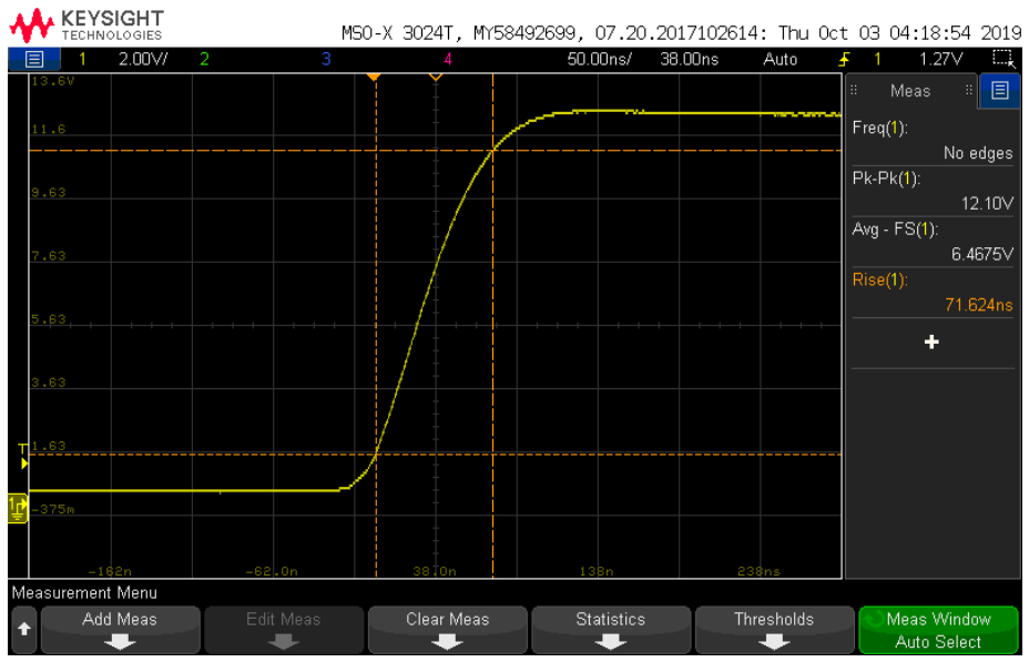
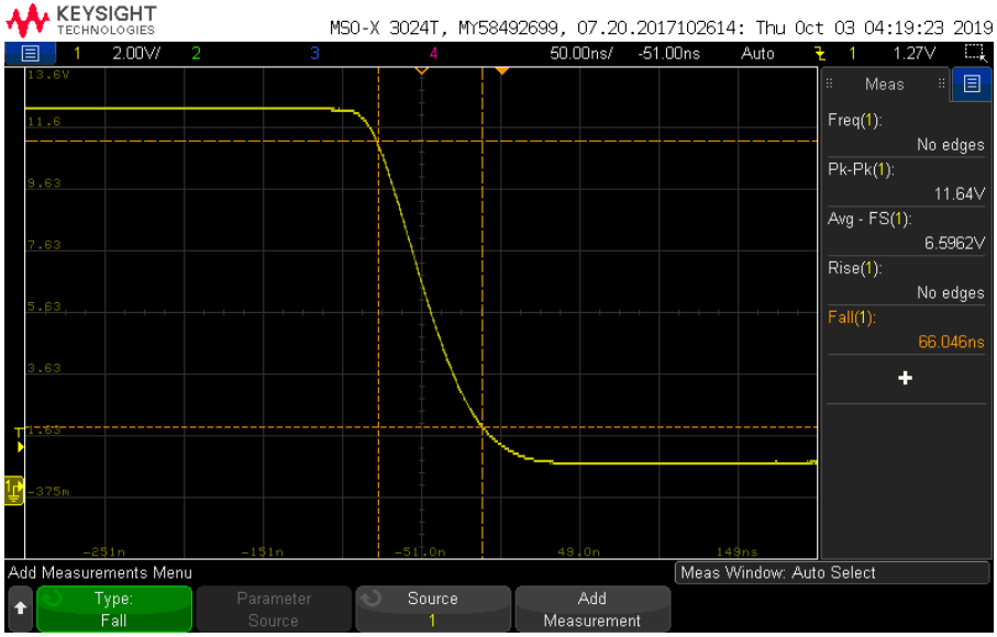
In the end, we were able to reach a rise time of 71.6 ns and a fall time of 66 ns. Certainly not breaking any records, but not all too bad.
Sawtooth Ramp Generator
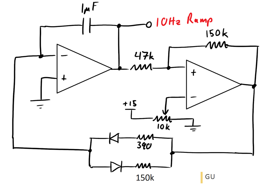
The frequency sweep function of our design was accomplished with a sawtooth oscillator. You’ll notice that this structure is very similar to our primary oscillator. Since the spec only required a single frequency for the sweep, we were able to do away with any voltage control and set our oscillator frequency to a fixed 10 Hz. We found that introducing two diodes to the feedback path let us enforce drastically different oscillation frequencies between the rising and falling cycle. Using this technique we were able to create a signal which rose slowly and fell quickly. We were able to tune the voltage at which the sweep resets with the 10k potentiometer attached to the inverting input of the second op amp.